- 您现在的位置:买卖IC网 > Sheet目录2009 > MAX5101BEUE+ (Maxim Integrated Products)IC DAC 8BIT TRPL R-R 16-TSSOP
MAX5101
+2.7V to +5.5V, Low-Power, Triple, Parallel
8-Bit DAC with Rail-to-Rail Voltage Outputs
_______________________________________________________________________________________
3
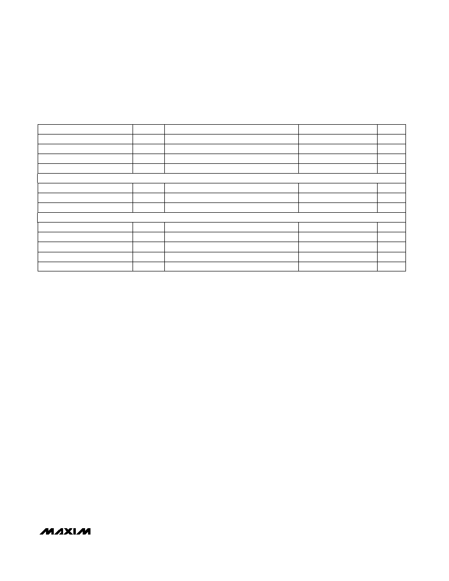
ELECTRICAL CHARACTERISTICS (continued)
(VDD = +2.7V to +5.5V, RL = 10k
, CL = 100pF, TA = TMIN to TMAX, unless otherwise noted. Typical values are at VDD = +3V and
TA = +25°C.)
Note 1: Reduced digital code range (code 00 hex to code F0 hex) due to swing limitations when the output amplifier is loaded.
Note 2: Gain error is: [100 (VF0,meas - ZCE - VF0,ideal) / VDD]. Where VF0,meas is the DAC output voltage with input code F0 hex, and
VF0,ideal is the ideal DAC output voltage with input code F0 hex (i.e., VDD 240 / 256).
Note 3: Output settling time is measured from the 50% point of the falling edge of WR to ±1/2LSB of VOUT’s final value.
Note 4: Channel-to-Channel Isolation is defined as the glitch energy at a DAC output in response to a full-scale step change on any
other DAC output. The measured channel has a fixed code of 80 hex.
Note 5: Digital Feedthrough is defined as the glitch energy at any DAC output in response to a full-scale step change on all eight
data inputs with WR at VDD.
Note 6: RL =
∞ , digital inputs at GND or VDD.
Note 7: Timing measurement reference level is (VIH + VIL) / 2.
CONDITIONS
UNITS
MIN
TYP
MAX
SYMBOL
PARAMETER
Digital-to-Analog Glitch Impulse
Code 80 hex to code 7F hex
90
nVs
Wideband Amplifier Noise
60
VRMS
Shutdown Recovery Time
tSDR
To ±1/2LSB of final value of VOUT
13
s
Time to Shutdown
tSDN
IDD < 5A
20
s
Power-Supply Voltage
VDD
2.7
5.5
V
Supply Current (Note 6)
IDD
280
520
A
Shutdown Current
13
A
Address to WR Setup
tAS
5
ns
Address to WR Hold
tAH
0
ns
Data to WR Setup
tDS
25
ns
WR Pulse Width
tWR
20
ns
Data to WR Hold
tDH
0
ns
POWER SUPPLIES
DIGITAL TIMING (Figure 1) (Note 7)
发布紧急采购,3分钟左右您将得到回复。
相关PDF资料
MAX5102AEUE+T
IC DAC 8BIT DUAL PAR-IN 16-TSSOP
MAX5104EEE+T
IC DAC 12BIT DUAL SER 16-QSOP
MAX5106EEE+T
IC DAC 8BIT QUAD NV 16-QSOP
MAX5109EEE+
IC DAC 8BIT DUAL NV 16-QSOP
MAX5138BGTE+T
IC DAC V-OUT 16BIT 1CH 16-TQFN
MAX514BEWI+
IC DAC 12BIT QUAD SER 28SOIC
MAX5150BCEE+
IC DAC 13BIT DUAL LP SER 16-QSOP
MAX5152ACEE+
IC DAC 13BIT DUAL LP SER 16-QSOP
相关代理商/技术参数
MAX5101BEUE+T
功能描述:数模转换器- DAC 8-Bit 3Ch Precision DAC RoHS:否 制造商:Texas Instruments 转换器数量:1 DAC 输出端数量:1 转换速率:2 MSPs 分辨率:16 bit 接口类型:QSPI, SPI, Serial (3-Wire, Microwire) 稳定时间:1 us 最大工作温度:+ 85 C 安装风格:SMD/SMT 封装 / 箱体:SOIC-14 封装:Tube
MAX5101BEUE-T
功能描述:数模转换器- DAC RoHS:否 制造商:Texas Instruments 转换器数量:1 DAC 输出端数量:1 转换速率:2 MSPs 分辨率:16 bit 接口类型:QSPI, SPI, Serial (3-Wire, Microwire) 稳定时间:1 us 最大工作温度:+ 85 C 安装风格:SMD/SMT 封装 / 箱体:SOIC-14 封装:Tube
MAX5102
制造商:MAXIM 制造商全称:Maxim Integrated Products 功能描述:+2.7V to +5.5V, Low-Power, Dual, Parallel 8-Bit DAC with Rail-to-Rail Voltage Outputs
MAX5102AEUE
功能描述:数模转换器- DAC RoHS:否 制造商:Texas Instruments 转换器数量:1 DAC 输出端数量:1 转换速率:2 MSPs 分辨率:16 bit 接口类型:QSPI, SPI, Serial (3-Wire, Microwire) 稳定时间:1 us 最大工作温度:+ 85 C 安装风格:SMD/SMT 封装 / 箱体:SOIC-14 封装:Tube
MAX5102AEUE+
功能描述:数模转换器- DAC 8-Bit 2Ch Precision DAC RoHS:否 制造商:Texas Instruments 转换器数量:1 DAC 输出端数量:1 转换速率:2 MSPs 分辨率:16 bit 接口类型:QSPI, SPI, Serial (3-Wire, Microwire) 稳定时间:1 us 最大工作温度:+ 85 C 安装风格:SMD/SMT 封装 / 箱体:SOIC-14 封装:Tube
MAX5102AEUE+T
功能描述:数模转换器- DAC 8-Bit 2Ch Precision DAC RoHS:否 制造商:Texas Instruments 转换器数量:1 DAC 输出端数量:1 转换速率:2 MSPs 分辨率:16 bit 接口类型:QSPI, SPI, Serial (3-Wire, Microwire) 稳定时间:1 us 最大工作温度:+ 85 C 安装风格:SMD/SMT 封装 / 箱体:SOIC-14 封装:Tube
MAX5102AEUE-T
功能描述:数模转换器- DAC RoHS:否 制造商:Texas Instruments 转换器数量:1 DAC 输出端数量:1 转换速率:2 MSPs 分辨率:16 bit 接口类型:QSPI, SPI, Serial (3-Wire, Microwire) 稳定时间:1 us 最大工作温度:+ 85 C 安装风格:SMD/SMT 封装 / 箱体:SOIC-14 封装:Tube
MAX5102BEUE
功能描述:数模转换器- DAC RoHS:否 制造商:Texas Instruments 转换器数量:1 DAC 输出端数量:1 转换速率:2 MSPs 分辨率:16 bit 接口类型:QSPI, SPI, Serial (3-Wire, Microwire) 稳定时间:1 us 最大工作温度:+ 85 C 安装风格:SMD/SMT 封装 / 箱体:SOIC-14 封装:Tube